
Open. Efficient. Scalable. The NPU for the AI Age.
ECATRON is a name forged from the ancient word EKA (ECA), meaning "the singular origin," combined with Tron, symbolizing a technological intelligence entity.
In a world rapidly shaped by artificial intelligence, ECATRON envisions a future where every device is intelligent and every region gains equal access to high-performance AI computing.
Making a chip has one gate that stops almost everyone: the mask. A mask set is ordered, paid for, and waited on, and changing a single line means ordering it again. ECATRON works where the mask is a file — a digital micromirror device projects the pattern straight onto the wafer, so a design revision takes an afternoon rather than a quarter.
Every layer beneath that sits on published, open material: process design kits from SkyWater, GlobalFoundries and IHP, a synthesis and layout chain with no licence to buy at any step, and 213 documented fabrication procedures. Breaking away from closed and monopolized semiconductor ecosystems is not a slogan here; it is the list of things we can hand you.
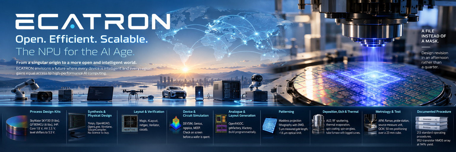
SkyWater SKY130 with nine standard cell and device libraries, GlobalFoundries GF180MCU with six, and IHP Open PDK. Core logic at 1.8 V, a high-voltage set at 3.3 V, and level shifters characterised to 5.5 V.
Yosys for synthesis, OpenROAD for place and route, OpenLane and librelane as the full flow, SiliconCompiler as the build system. No licence to buy at any step.
Magic for layout, KLayout for mask verification, netgen for layout-versus-schematic, Verilator and cocotb for register-transfer simulation.
DEVSIM and Genius for device physics, ngspice for circuits, MEEP for photonics. A design is checked on screen before a wafer is spent.
OpenFASOC generates analogue blocks from specification. gdsfactory and kfactory build layout programmatically rather than by hand.
Maskless projection lithography built from a digital micromirror device. Measured gate length today is 5 micrometres; the optical limit of the current optic sits near 1.6 micrometres.
Atomic layer deposition, RF sputtering with impedance matching, thermal evaporation, spin coating, spin-on-glass, and a tube furnace with logged oxidation curves.
Atomic force microscopy, Raman spectroscopy, a probe station, a source-measure unit, and a quartz crystal thickness monitor. A positioning stage resolves 50 nanometres over a 23 millimetre cube.
213 standard operating procedures covering every step above. A measured NMOS array of 952 transistors came out at 94% yield.
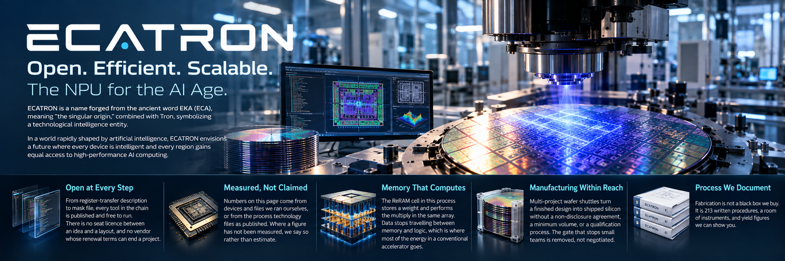
From register-transfer description to mask file, every tool in the chain is published and free to run. There is no seat licence between an idea and a layout, and no vendor whose renewal terms can end a project.
Numbers on this page come from devices and files we ran ourselves, or from the process technology files as published. Where a figure has not been measured, we say so rather than estimate.
The ReRAM cell in this process stores a weight and performs the multiply in the same array. Data stops travelling between memory and logic, which is where most of the energy in a conventional accelerator goes.
Multi-project wafer shuttles turn a finished design into shipped silicon without a non-disclosure agreement, a minimum volume, or a qualification process. The gate that stops small teams is removed, not negotiated.
Fabrication is not a black box we buy. It is 213 written procedures, a room of instruments, and yield figures we can show you.
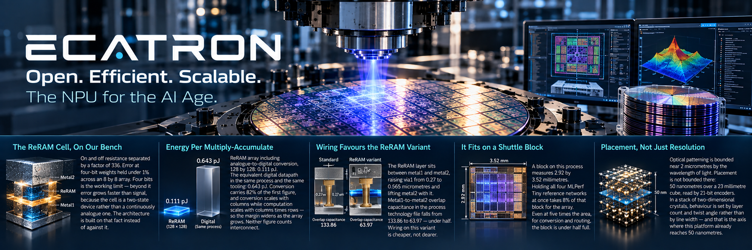
On and off resistance separated by a factor of 336. Error at four-bit weights held under 1% across an 8 by 8 array. Four bits is the working limit — beyond it error grows faster than signal, because the cell is a two-state device rather than a continuously analogue one. The architecture is built on that fact instead of against it.
ReRAM array including analogue-to-digital conversion, 128 by 128: 0.111 pJ. The equivalent digital datapath in the same process and the same tooling: 0.643 pJ. Conversion carries 82% of the first figure, and conversion scales with columns while computation scales with columns times rows — so the margin widens as the array grows. Neither figure counts interconnect.
The ReRAM layer sits between metal1 and metal2, raising via1 from 0.27 to 0.565 micrometres and lifting metal2 with it. Metal1-to-metal2 overlap capacitance in the process technology file falls from 133.86 to 63.97 — under half. Wiring on this variant is cheaper, not dearer.
A block on this process measures 2.92 by 3.52 millimetres. Holding all four MLPerf Tiny reference networks at once takes 8% of that block for the array. Even at five times the area, for conversion and routing, the block is under half full.
Optical patterning is bounded near 2 micrometres by the wavelength of light. Placement is not bounded there: 50 nanometres over a 23 millimetre cube, read by 21-bit encoders. In a stack of two-dimensional crystals, behaviour is set by layer count and twist angle rather than by line width — and that is the axis where this platform already reaches 50 nanometres.
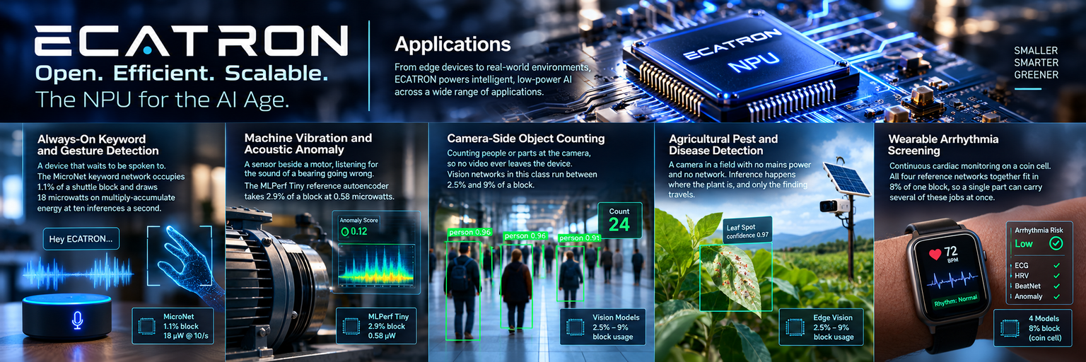
A device that waits to be spoken to. The MicroNet keyword network occupies 1.1% of a shuttle block and draws 18 microwatts on multiply-accumulate energy at ten inferences a second.
A sensor beside a motor, listening for the sound of a bearing going wrong. The MLPerf Tiny reference autoencoder takes 2.9% of a block at 0.58 microwatts.
Counting people or parts at the camera, so no video ever leaves the device. Vision networks in this class run between 2.5% and 9% of a block.
A camera in a field with no mains power and no network. Inference happens where the plant is, and only the finding travels.
Continuous cardiac monitoring on a coin cell. All four reference networks together fit in 8% of one block, so a single part can carry several of these jobs at once.
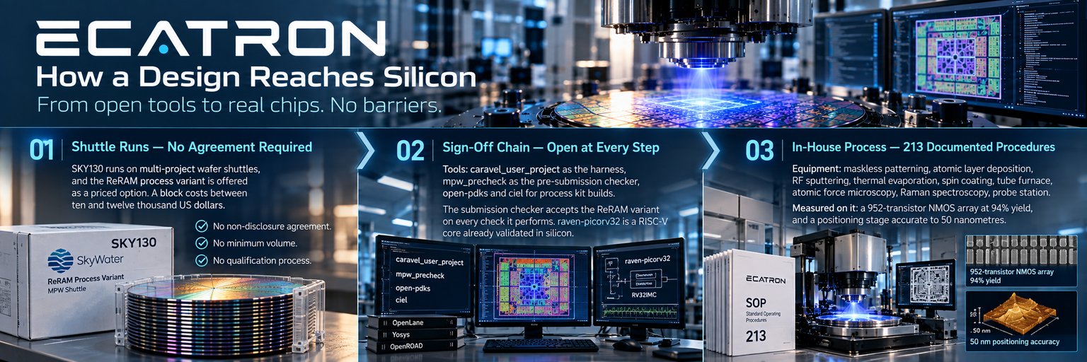
SKY130 runs on multi-project wafer shuttles, and the ReRAM process variant is offered as a priced option. A block costs between ten and twelve thousand US dollars.
No non-disclosure agreement. No minimum volume. No qualification process.
Tools: caravel_user_project as the harness, mpw_precheck as the pre-submission checker, open-pdks and ciel for process kit builds.
The submission checker accepts the ReRAM variant on every check it performs. raven-picorv32 is a RISC-V core already validated in silicon.
Equipment: maskless patterning, atomic layer deposition, RF sputtering, thermal evaporation, spin coating, tube furnace, atomic force microscopy, Raman spectroscopy, probe station.
Measured on it: a 952-transistor NMOS array at 94% yield, and a positioning stage accurate to 50 nanometres.
"Open. Efficient. Scalable. The intelligence layer that powers every ÁRKMORA innovation at the edge of civilization."
ECATRON — The NPU for the AI Age.